Bench Power Supply
Summary
Together with two friends, we designed a dual-channel floating bench power supply for the Electronics Workshop course at Aalto University. The course provided facilities for designing and executing an electronics project over the course of a semester. We designed everything from the analog and digital circuits to the enclosure.
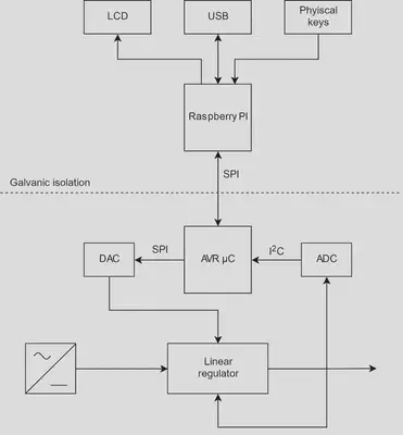
Both of the power supply output channels are independent, and have their own galvanically isolated control system. The user interface is running on a Raspberry Pi, which communicates with the power supply channels through an SPI connection through optocouplers.
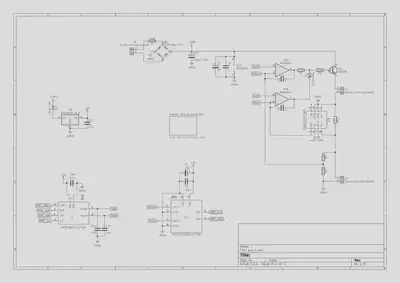
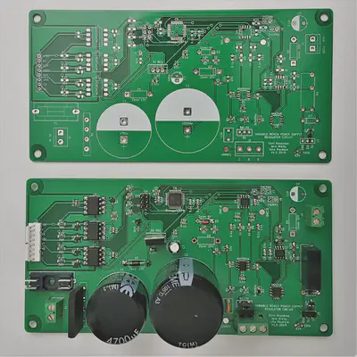
- Designed the regulator PCB and two interface PCBs from scratch using KiCAD.
- We tried out as many PCB manufacturing techniques as possible, including acid etching, CNC routing and we had the regulator PCBs professionally manufactured (not including assembly).
- Regulator firmware for the AVR microcontroller.
- Interface software for Raspberry Pi.
- Physical user interface software as a USB HID.
- Evaluated the finished power supply against a commercial power supply with similar specifications.
Introduction
The subject of the project was an adjustable laboratory power supply. Based on the specification, we set out to build a laboratory power supply with a digitally adjustable voltage between 0-24V and a current of 0-2A. The specification changed slightly from the design, as the transformer we chose gives up to 3A power to the two channels. The voltage and current of the final device are adjustable between 0-24V and 0-3A.
Implemented hardware
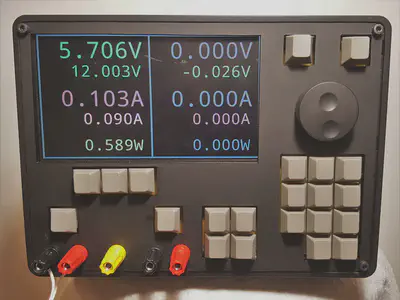
Features:
- Two galvanically isolated output channels
- Voltage range: 0-24V / channel, 48V if connected in series
- Current range: 0-3A / channel, 6A if connected in parallel
- Power: 144W
- Voltage accuracy: ≈ 50mV
- Current accuracy: ≈ 10mA
- Outputs: Two / channel, and one for ground
- Inputs: C13 connector 230V
- Overheating protection
- Current limitation
- Temperature-controlled fan
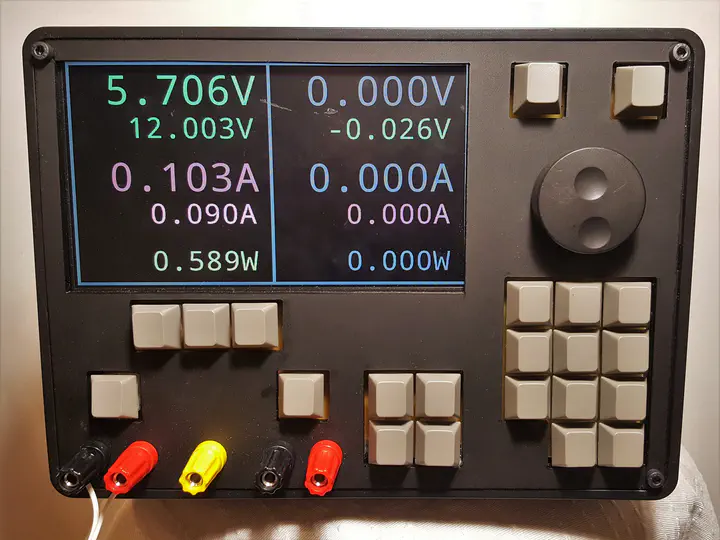
- 7” LCD display
- Keypad and rotary encoder for adjusting settings
- Controllable through USB
The operation of the device is controlled by a single-board computer Raspberry Pi Zero. The user interface is displayed on a 7” LCD and the device can be controlled through either physical keys or over USB.
Linear Regulator
The Raspberry Pi controls two identical regulator circuits using SPI. One such circuit is illustrated in the block diagram below the galvanic isolation line. The circuit has an AVR microcontroller which receives the desired voltage and current limits from the Raspberry Pi. The microcontroller then sends the received voltage and current limits to the DA converter and reads the realized voltage and current from the AD converter. Each circuit has its own optical isolators for the SPI bus and the operating voltages of both circuits are galvanically isolated from each other and from ground. The Raspberry Pi also controls the output relays to disconnect the load if necessary.
The main components of the regulators are:
| Component | |
|---|---|
| Operational Amplifier | MAX9944ASA+T |
| Analog to Digital Converter (ADC) | MCP3422A0-E/SN |
| Digital to Analog Converter (DAC) | MCP4822-E/SN |
| Current Amplifier | INA240A1DR |
| Microcontroller | ATMEGA328PB-AU |
The circuit is switched on when a 25-28V (rms) AC voltage is connected to connector J1. The AC voltage is rectified and filtered with a 15000uF electrolytic capacitor. The microcontroller monitors the operating voltage through the UNREG_MON pin connected to the ADC. This signal is reduced and overvoltage-protected.
U2 provides the 5V supply voltage for the microchips requiring it. In order to keep the power dissipated in the regulator reasonable, a 15V zener diode is placed between it and the operating voltage, which dissipates approximately half of the power. The operational amplifier U1 controls the transistor on the high voltage side of the load, which means it operates in a large voltage range and is connected directly to the rectifier through the overvoltage protection formed by the zener diode D3.
The output voltage of the power supply is measured through the voltage divider formed by R6 and R7 and the current is measured through a separate current amplifier U3. These provide the reference voltages of the operational amplifiers as well as the signals measured by the AD converter.
The voltage adjustment is implemented using the operational amplifier U1A. U1A compares the measured and the set voltage to each other, and adjusts the base voltage of output transistor Q1 accordingly. In current control mode, the operational amplifier U1B compares the set and measured current. When the measured value is higher than the set value, the operation amplifier pulls down the voltage at the output transistor through the Schottky diode D4, until the measured current corresponds to the set value. Otherwise, the operational amplifier supplies maximum voltage to its output and no current flows through the diode.
Several measures have been taken to improve noise suppression. Every microchip has a corresponding 0.1uF bypass capacitor to minimize high frequency interference in the power supply output. Low-pass filters are installed at the outputs of the DA converter to reduce noise in said output. The output noise is also significantly reduced by the capacitors added between the inverting input and output of the operational amplifiers.
Microcontroller firmware
The microcontroller receives commands from the user interface over the SPI bus, and communicates with the DA and AD converters over I2C and SPI buses. Because the SPI bus between the UI and microcontroller is bidirectional, the values read by the ADC are always sent to the UI when a command arrives. The firmware is implemented using C and the C standard library (avr-libc), and uses interrupts for simultaneous use of multiple data buses. The source code is located in the “control_mc” directory on Github.
Front panel
The front panel of the device consists of a 7” LCD display, a rotary encoder, mechanical keys and connectors for channel outputs and ground. The LCD screen is connected to the Raspberry Pi through HDMI. The keys are monitored by a Arduino Pro Micro microcontroller, which operates a standard HID USB keyboard for the Raspberry Pi using qmk-firmware.
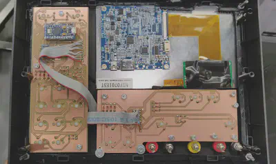
The front panel keys and the rotary encoder switch are connected in a 5x5 matrix using diodes. The microcontroller scans the switch matrix and reads the rotation of the rotary encoder.
As shown in the figure, the front panel switches are divided into two circuit boards, between which the rows and columns of the matrix are connected by wires.
Measurements and testing
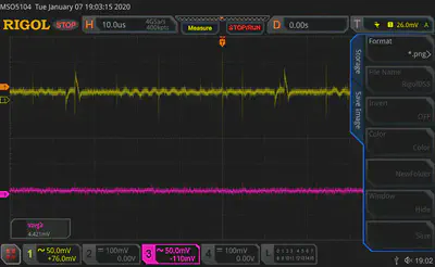
We tested the performance of our device by measuring the output with an oscilloscope and comparing the result with the linear power supply DF1731SB found at the workshop. The tests measured two different idle voltages, the voltage under load, and the voltage stability as the load changed.
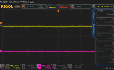
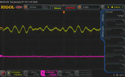
The no-load voltage was measured at the set values of 2.5V and 20V. In both cases, significant noise was emitted from our device compared to the reference power supply. Noise occurred at about 20kHz. This information could be used to reduce noise by adding or adjusting filter capacitors.
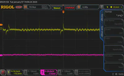
When measuring the output with a load, we used a power resistor of about 4 ohms. Measurements were made with both voltage and current control limiting output 1A current. With voltage limitation, our device worked well, but with current limitation, the result is significantly worse.
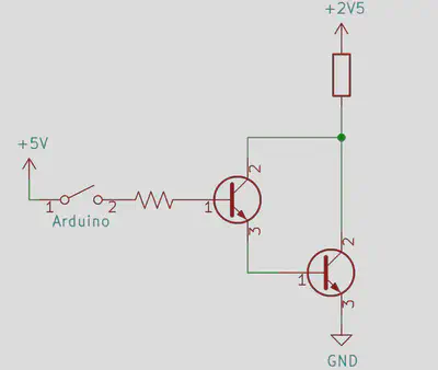
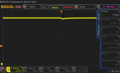
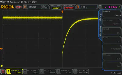
To measure the effect of a load change, we used the circuit below, which connects a 4-ohm load to a device set to 2.5V at idle. The circuit was implemented without mechanical switches to minimize interference to the measurement.
The result is much worse than the reference power supply. This is significantly affected by the capacitance at the output of the power supply, which is not added in our own device. This capacitance, on the other hand, would slow down operation if the voltage were to change rapidly, especially in constant current mode.
Conclusions
Our initial specification called for a voltage range of 0-24V and current range of 0-2A. The ranges of the realized device is 0-24V and 0-3A per channel. We ended up making two identical galvanically separated channels in the device, which can be connected in series so that the voltage can be adjusted between 0-48V. The channels can also be connected in parallel, giving up to 6A of current. The planned power was 2 x 48W and the actual power is 2 x 72W = 144W. The project went well and met our requirements specification, and even exceeded it in terms of performance. Based on the tests, the device could be improved by increasing the output capacitance and reducing interference with better filtering.